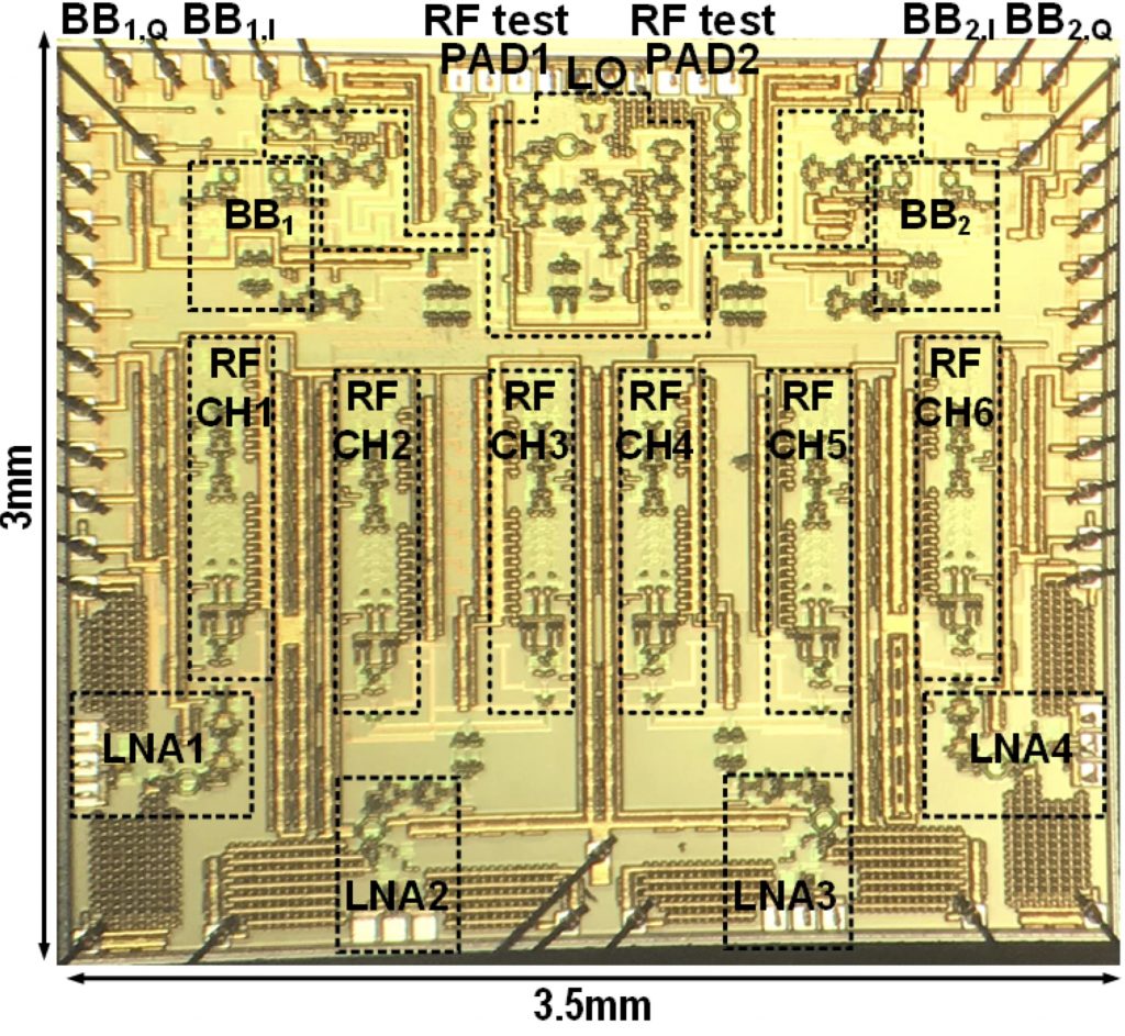
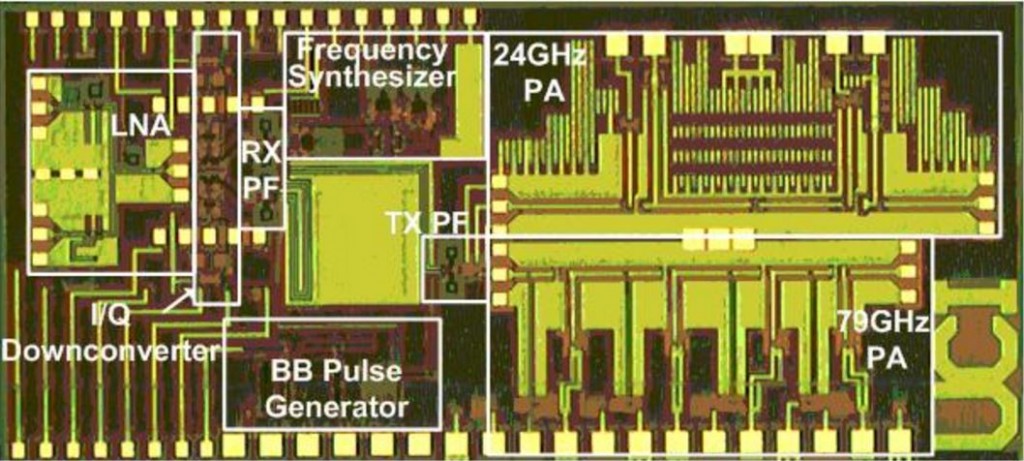
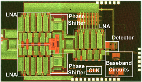
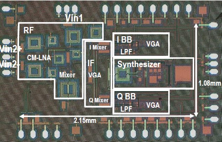
A dual-band 22-29-GHz/77-81-GHz BiCMOS transceiver for automotive radars
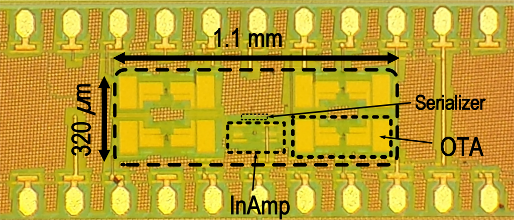
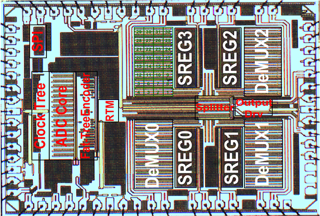
A 4-bit 12GS/s data acquisition System-on-Chip including a Flash ADC and 4-Channel DeMUX in 130nm CMOS
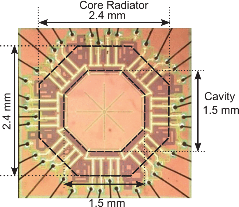
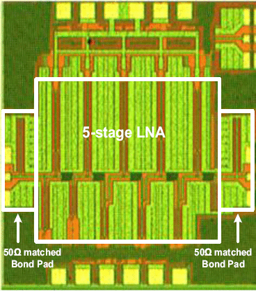
A 94-GHz Passive Imaging Receiver using a Balanced LNA with Embedded Dicke Switch in 180nm SiGe BiCMOS
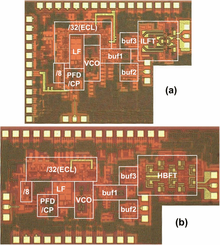
(a) A PLL using an injection-locked frequency tripler and (b) a PLL using harmonic-based frequency tripler in 0.18μm SiGe BiCMOS for 96GHz frequency generation
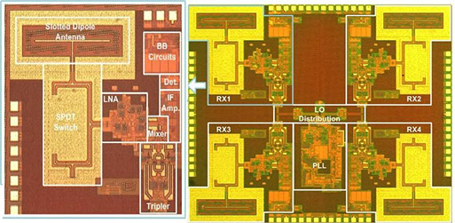
A Zero-IF W-band Front-End Receiver with Frequency Tripler
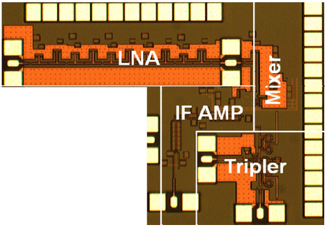
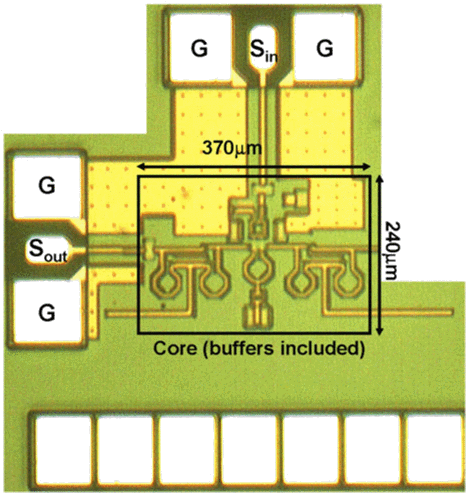
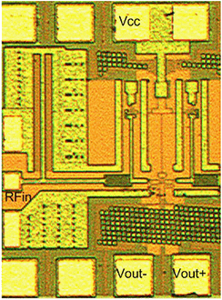
A W-band LNA in 0.18-μm SiGe BiCMOS
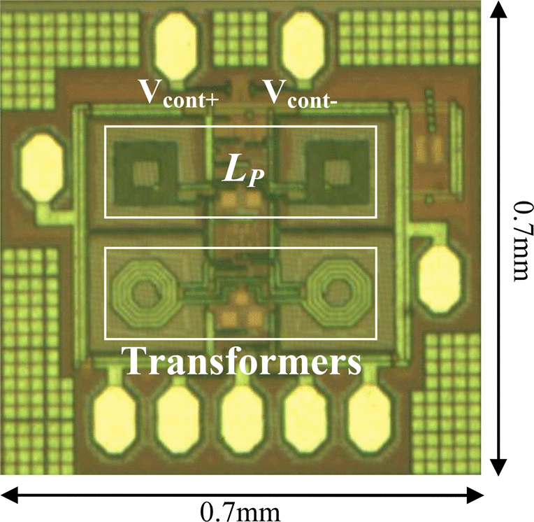
A W-band Transformer-Based Injection-Locked Frequency Tripler in 65nm CMOS
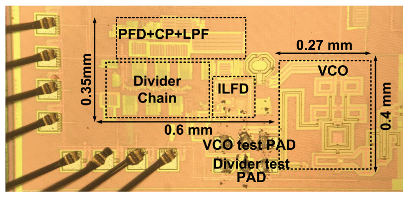
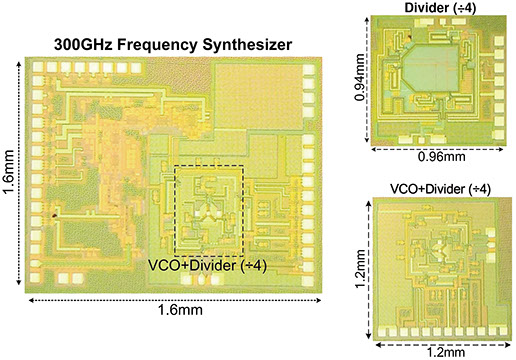
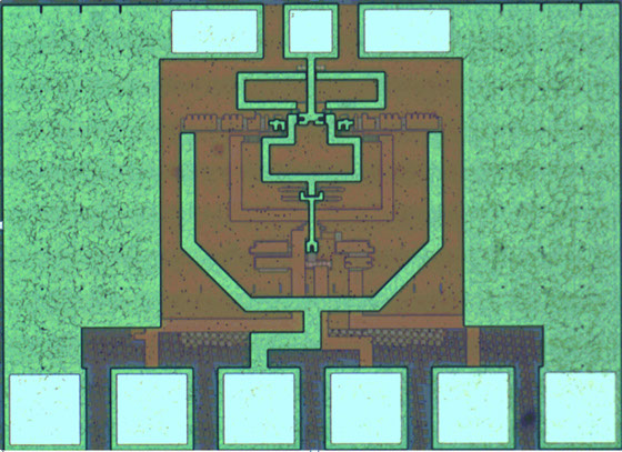
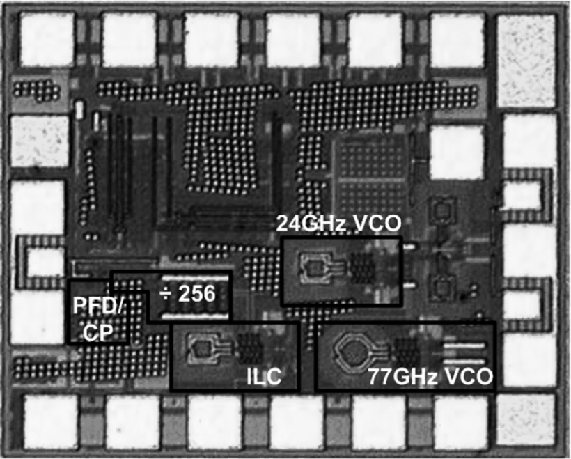
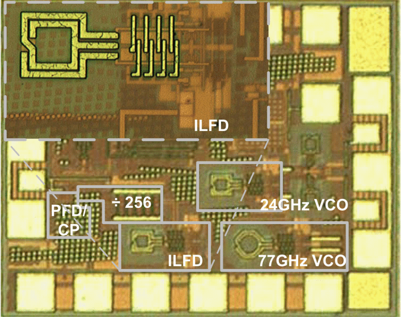
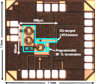
A millimeter-wave dual-band frequency synthesizer, operating in the 24 GHz and 77 GHz bands in 180nm SiGe BiCMOS
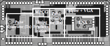
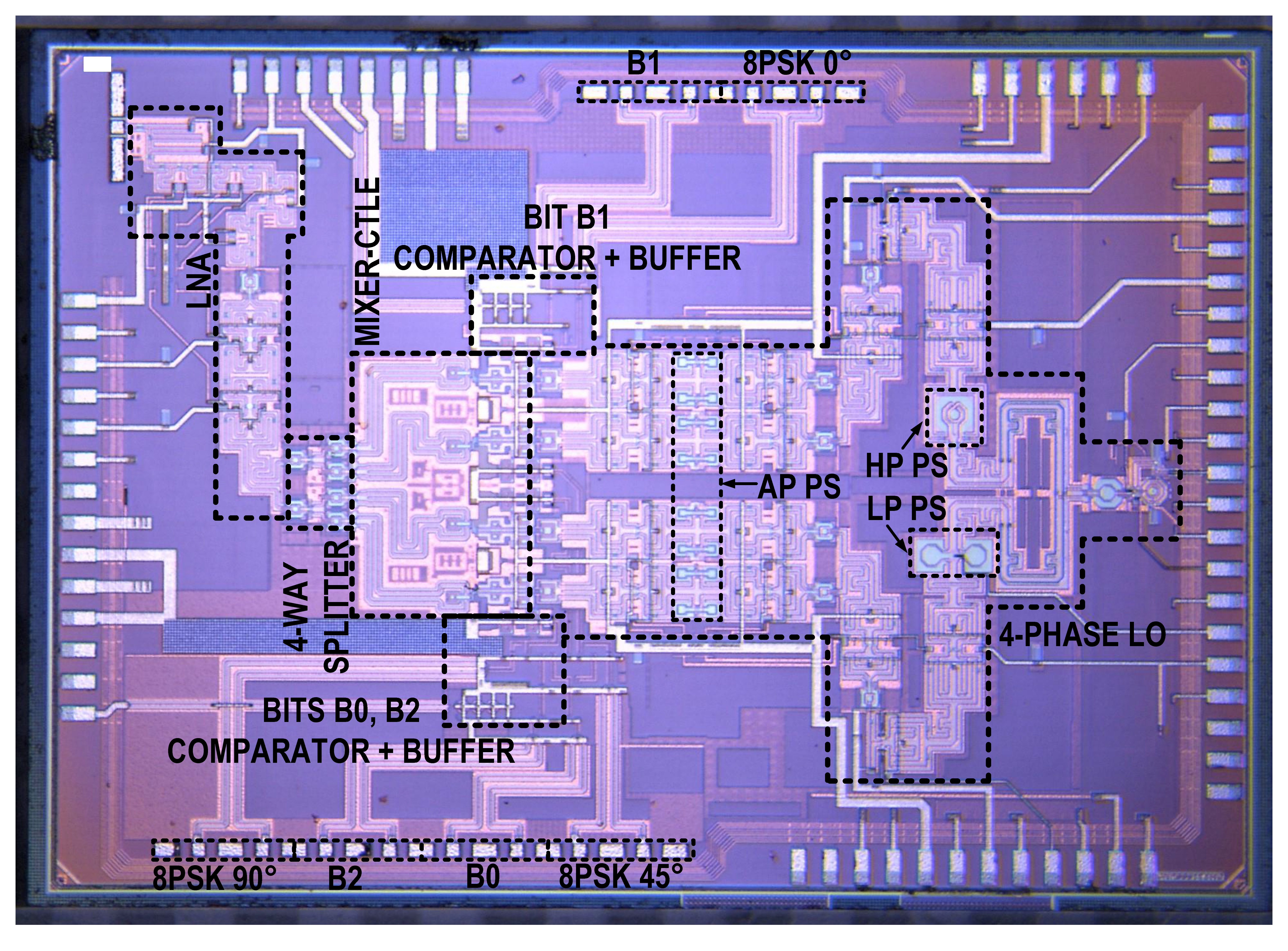
A distributed active power splitter for a multi-antenna UWB transceiver in 130nm CMOS