Terahertz (THz) Integrated Circuits for Imaging, Sensing, and Communications
(Sponsors: NSF and JPL)
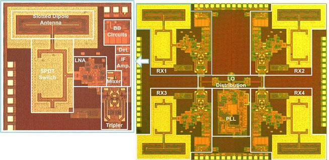
The vastly under-utilized spectrum in the THz frequency range enables disruptive applications including 10-gigabit chip-to-chip wireless communications and imaging/spectroscopy. On the imaging applications front, THz imaging is considered to be one of the emerging and disruptive technologies over the next decade [1]. As stated in that article: “great things are expected of terahertz waves in ranging from 0.3-3THz.” THz waves pass through non-conducting materials such as clothes, paper, wood and brick and so cameras sensitive to them can peer inside envelopes, into living rooms and “frisk” people at distance. THz imaging systems, therefore, will be key enabling components in applications such as security surveillance (to find concealed weapons and explosives), non-destructive testing, biology, radio astronomy, and medical imaging. On the sensing and communications, the absence of licensed frequency spectrum in the THz frequency range makes it possible to explore new unprecedented ideas on super-precise sensing at micrometer-level and multi-10-gigabit instant wireless access at the centimeter-level spacing between transmitter and receiver.
- Zheng Wang, Pei-Yuan Chiang, Peyman Nazari, Chun-Cheng Wang, Zhiming Chen, and Payam Heydari, “A 210 GHz Fully Integrated Differential Transceiver with Fundamental Frequency VCO in 32 nm SOI CMOS,” IEEE Int’l Solid-State Circuits Conference (ISSCC), Feb. 2013.
- Pei-Yuan Chiang, Omeed Momeni, and Payam Heydari, “A Highly Efficient 0.2 THz Varactor-Less VCO with -7dBm Output Power in 130nm BiCMOS,” IEEE Compound Semiconductor IC Symp. (CSICS), Oct. 2012.
- Francis Caster, II, Leland Gilreath, Shiji Pan, Zheng Wang, Filippo Capolino, and Payam Heydari, “A 93-113GHz BiCMOS 9-Element Imaging Array Receiver Utilizing Spatial-Overlapping Pixels with Wideband Phase and Amplitude Control,” IEEE Int’l Solid-State Circuits Conference (ISSCC), Feb. 2013.
Brain-Computer Interface
(Sponser: NSF)
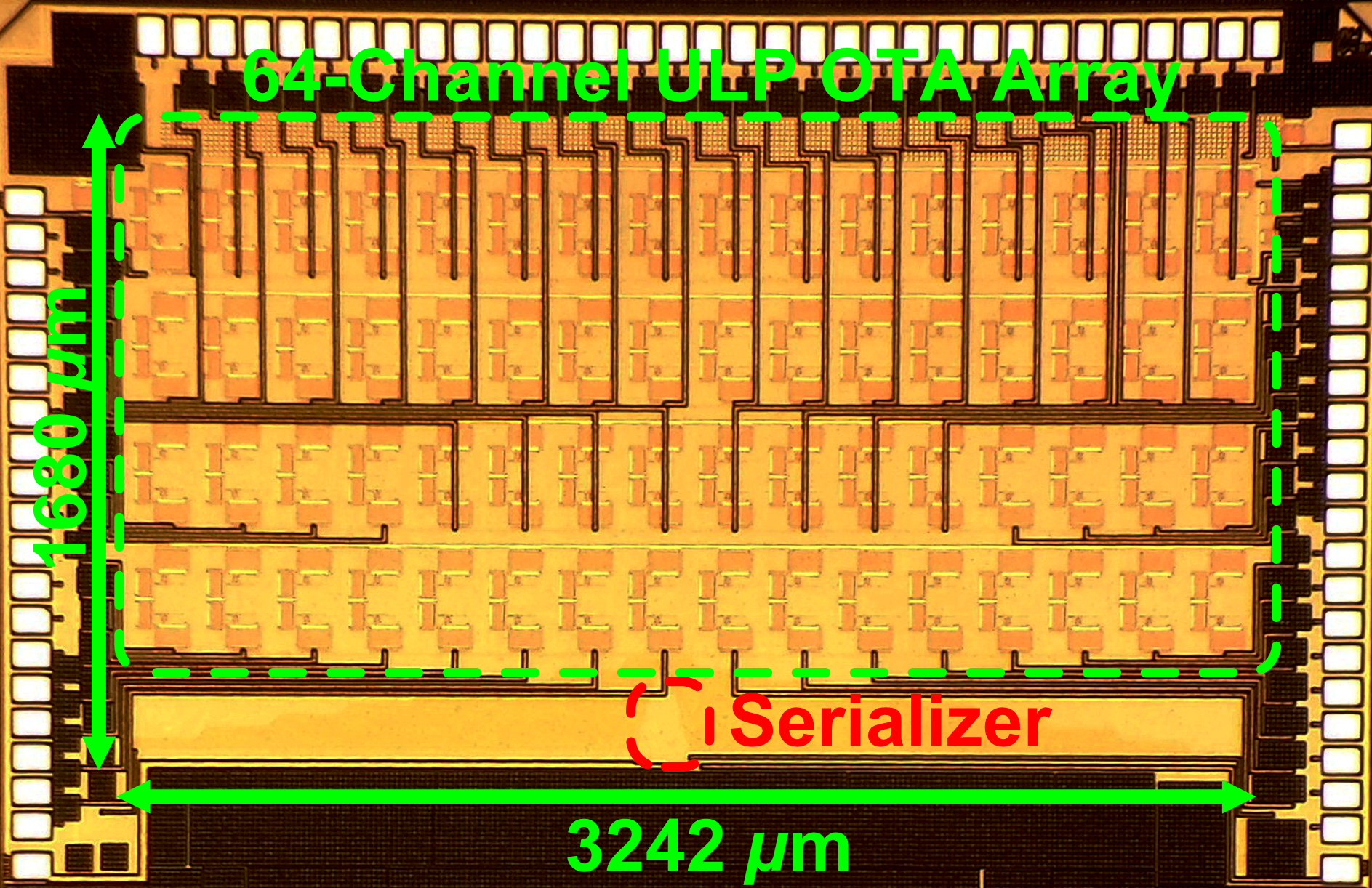
Brain-computer interfaces (BCIs) are systems that record brain activity in real time, decode movement intentions from these activity patterns, and use this information to operate end-effectors, such as robotic orthoses or muscle stimulators. The research vision is to design a miniaturized BCI system that is safe for human implantation and capable of restoring movements to individuals paralyzed due to SCI, stroke, or other neurological injuries. BCI system will reconnect the brain with the muscles, thereby providing a technological solution to restoring the much-sought-after able-bodied motor function to those affected by SCI, stroke, or other neurological injuries.

Electro-Optic Phased-Array and Passive/Active Imaging Systems
(Sponsors: NSF)
The objective of this research is to:
- Develop and investigate a new low-cost, broadband, RF-modulated near-infrared imaging integrated system for detecting breast cancer. The approach is to design a novel electro-optic two-element phased-array system with high spatial resolution to obtain accurate information about the breast tissue’s optical scattering and absorption properties.
- Develop fully integrated passive/active imaging systems with on-chip antennas, while leveraging high level of integration offered by Silicon technologies.

Silicon-Based (Sub)-Millimeter-Wave IC Design
(Sponsors: SRC, Industry)
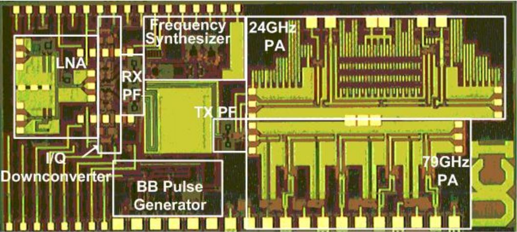
Research and development of silicon-based solutions for millimeter-wave (MMW) applications has gained significant momentum in recent years. These applications include 60-GHz short-range high data-rate communications, automatic cruise control (ACC) and collision-avoidance systems using 24/77-GHz automotive radars, and more recently, 94-GHz/140-GHz security and medical applications using passive imaging. The goal of this research is to design fully integrated transceivers for automotive radars and imaging systems.

Ultra Wideband RF IC Design
(Sponsors: NSF, Industry)
Ultra Wide-band (UWB) wireless radios are capable of carrying extremely high data rates for up to 250 feet with little transmit power, and high immunity to interference and noise. Furthermore, the spread spectrum characteristics of UWB wireless systems, and the ability of the UWB wireless receivers to resolve the multipath fading due to the nature of the wireless impulse transmission, make UWB systems a promising wireless for a variety of high-rate, short- to medium-range wireless communications. The design of the RF frond-end blocks including frequency synthesizers on both transmitter and receiver sides, and low noise amplifier (LNA)/mixer on the receiver side with bandwidths in excess of 500 MHz is very challenging. Our goal is to explore new design techniques and novel circuit architectures to design the front-end RF circuits including the UWB LNA, mixer, power amplifier, and frequency synthesizer.
Selected publications:
- Payam Heydari, “A Comprehensive Study of Low-Power Ultra Wideband Radio Transceiver Architectures,” IEEE Wireless Communications & Networking Conference (WCNC), March 2005.
- Amin Q. Safarian, Ahmad Yazdi, Payam Heydari, “Design and Analysis of an Ultra Wide-band Distributed CMOS Mixer,” IEEE Trans. on VLSI Systems, no. 5, vol. 13, pp. 618-629, May 2005.
- Payam Heydari, Denis Lin, Amin Shameli, Ahmad Yazdi, “Design of CMOS Distributed Circuits for Multiband UWB Wireless Receivers,” IEEE RF IC Symposium, 2005.
- Payam Heydari and Denis Lin, “A Performance Optimized CMOS Distributed LNA for UWB Receivers,” IEEE Custom Integrated Circuits Conference (CICC), Sept. 2005.

Ultra High-Speed Broadband IC Design
(Sponsors: NSF, Industry)
Various broadband wireline transmission standards have evolved for specific applications, including: (1) Optical Network (SONET) used in wide-area networks for long-haul (50-100km) transmission over fiber and (2) 10-Gigibit Ethernet, used for short- and medium-range communication over optical fiber, as well as short serial back-plane connections over copper. Although these protocols differ in higher-level data processing (e.g., framing), the requirements on the physical layer signal processing are similar for all of them. In particular, the system jitter and noise requirements in these broadband systems pose a number of challenges in the design of the electronic blocks. Operations such as equalization, serialization/deserialization, clock multiplication, and clock recovery are usually done electronically at the desired bit rates – 40Gb/s and higher up to 80Gb/s– require sufficiently accurate timing in the data transitions. Equally important is that the design of front-end high-speed circuits, including the transimpedance amplifier (TIA), laser driver, and channel equalizer, requires a comprehensive knowledge of the channel behavior. In the case of optical transceivers, the research efforts must build a bridge between the optical communications and advanced high-speed IC design.
Selected publications:
- Ahmad Yazdi, Denis Lin, Payam Heydari, “A 1.8V Three-Stage 25GHz 3dB-BW Differential Non-Uniform Downsized Distributed Amplifier,” IEEE International Solid-State Circuits Conference (ISSCC), Feb. 2005.
- Ravindran Mohanavelu and Payam Heydari, “A Novel Flip-Flop-Based Frequency Divider in 0.18um CMOS,” IEEE European Solid-State Circuits Conference (ESSCIRC), Sept. 2005.

Noise and Signal Integrity in High-Speed Mixed-Signal VLSI Circuits
(Sponsor: NSF)
Noise is a crucial problem in modern mixed-signal VLSI circuits and is becoming increasingly important as the minimum feature size shrinks to 0.13 micron and below. Noise sources are either internal to the devices (e.g., shot noise, 1/f noise, and thermal noise), or external sources (e.g. bounce noise, crosstalk noise, and charge sharing noise). Due to their higher magnitude and energy, the external noise sources play a more important role in determining the circuit reliability and performance.
Power/ground noise, crosstalk, and substrate noise are major external noise sources that can have harmful effects on the circuit performance and reliability. For example, they can cause false switching in the logic gates especially dynamic logic gates, timing failures due to setup and hold time violations, and timing jitter in the on-chip clock generators. The goal of this research is to analysis power/ground noise, crosstalk, and substrate noise in mixed-signal VLSI circuits. We further focus on the effect of power/ground noise and substrate noise on the timing jitter of CMOS phase-locked loops (PLLs) and delay-locked-loops (DLLs).
Selected publications:
- Payam Heydari, “Analysis of the PLL Jitter Due to Power/Ground and Substrate Noise,” IEEE Trans. on Circuits and Systems I, no. 12, vol. 51, pp. 2404-2416, Dec. 2005. (Recipient of IEEE Circuits and Systems Society Darlington Best Paper Award)
- Payam Heydari, “Characterizing the Effects of the PLL Jitter Due to Substrate Noise in Discrete-Time Delta-Sigma Modulators,” IEEE Trans. on Circuits and Systems I, 2005.